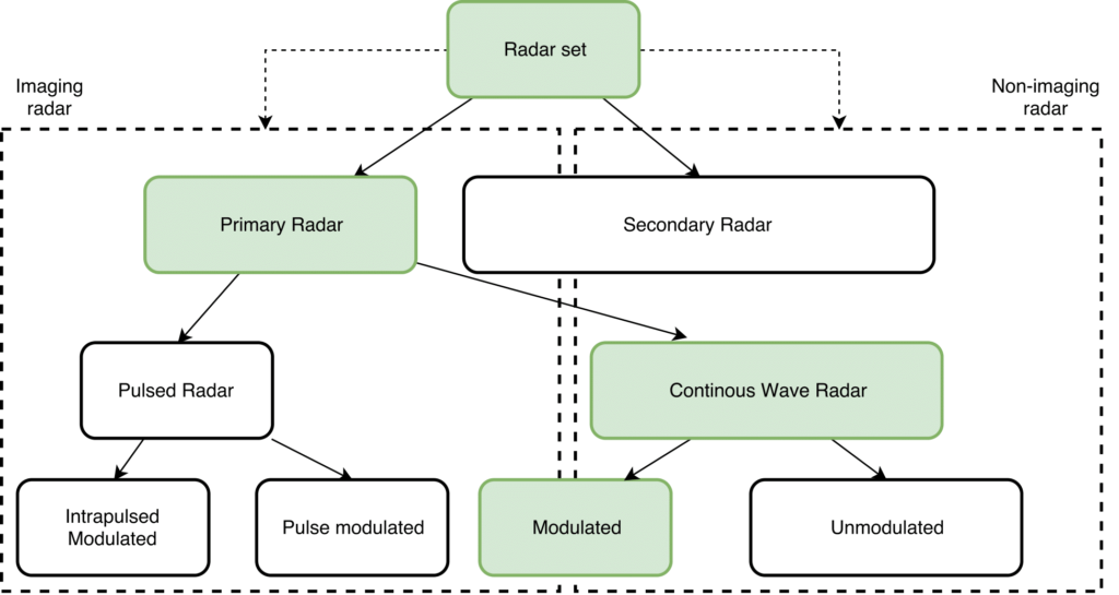
S Band Microwave Sensor
- Ashish Kumar Jha
- Subha Sarkar
- Tushar Kumar
Dr. Yogendra Kumar Prajapati
Assistant Professor
MNNIT Allahabad
Contact : yogendrapra.mnnit.ac.in
1st Prototype – January 2018 – April 2018 (scheduled)
Note : This project was partially done as some of the hardware design under-performed.
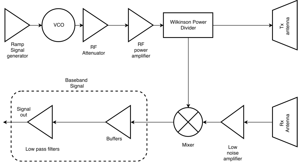
Short Range Microwave radar is a continuously growing field of research in field of robotics and automotive. These microwave radar are being actively used to develop highly reliable sensors for Advanced Driver Assistance System (ADAS) in Automotive industry. The signal used for finding ranges in radar systems is an electromagnetic (EM) wave at microwave frequencies. The main advantage of radar systems compared to other alternatives such as sonar and LiDAR is the immunity to weather conditions and potential for lower cost realisation. It requires a directional radar, RF front-end, compact & low-power DSP computer to implement the sensor.
Motivation and Inspiration
Radar has long been used in meteorology and military applications. Recently Radar has begun to appear on high-end automobiles for parking assistance and lane departure warning. Next-generation automotive and robotic radars are expected to provide adaptive cruise control and active collision avoidance.
We saw the project at MIT Lincoln Laboratory where a synthetic aperture radar was made using Mini-Circuits modules. Here we are trying to design such radar system using ICs and study the performance the system. Due to complexity of the design, we will limit our problem to design of stationary radar with stationary objects.
Radar Link Budget
Radar performance is governed by the link budget equations, which determines what levels of signals are available for detection. A simplified version of the link budget equation is given below :
\[P_r = \frac{P_tG^2\sigma{}\lambda^2\tau}{(4\pi)^3R^4}\]
\(P_t\) = Peak transmit power = \(15dBm\) = \(31.6mW\)
\(G\) = (Assuming similar antennas) Gain of the antenna = \(10dB\) = \(10\)
\(\sigma\) = Radar cross section or area of the target = \(1m^2\)
\(\lambda\) = Radar wavelength (assuming center frequency to be 2.5GHz) = \(12cm\)
\(\tau\) = Duty cycle of the transmitter = \(1\) (CWFM)
\(R\) = Range of the target = \(1m\) to \(40m\)
Putting the values of maximum range and minimum range we obtain \(P_{r,min}\) = \(8.957\times{10^{-12}}W\) = \(-80.478dBm\) and \(P_{r,max}\) = \(2.29\times{10^{-5}}W\) = \(-16.39dBm\)
Range resolution
Estimating Noise floor
The round trip delay (\(\tau = 2R/c\)) for a target at 20m = 133.3ns
For a target at 2m = 6.67ns
For a frequency being ramped up @ 1KHz/ns (arbitrary chosen), the offset generated would be 133.3KHz and 6.67KHz. For limiting the hardware resources, we choose 2048 point FFT. It depends on the hardware capability we are using. We are deploying Cyclone V SoC for this. We are using HMC385 (VCO) for generating carrier.

If the \(V_{tune}\) ranges from 1V to 9V (For maximum linearity), then the bandwidth would be 300MHz (2.55GHz – 2.25GHz). If the ramp up time (\(T\)) is 0.3ms we get the value of 1KHz/ns rate. So to get 2048 points (for FFT) in 0.3 seconds the required sampling rate should be 6826666.67 samples/second or ~ 6.8MSPS.
The Bandwidth of the system is \(\frac{1}{T}\). In the interval of \(T\), the noise accumulates in the system and hence becomes the effective noise bandwidth.
The noise floor is estimated by :
\[N_{floor} = 10\log(k\times{T_0}\times{1000}) + NF + 10\log(BW)\]
\(T_0\) = \(290K\)
\(NF\) = \(10dB\)(Noise figure of receiver)
\(BW\) = \(3333.33 Hz\) = \(\frac{1}{T}\)
So, the \(N_{floor}\) comes to be \(-128dBm\). However this is quite optimistic result. There would some otherr sources of random noise from transmission lines, antenna and power supplies which may increase the noise floor. Let’s assume the noise floor be at -120dBm.
Choosing an ADC
The SNR for the weakest signal from target at 40m is found to be \(P_{r,min}-N_{floor} = -80.478dBm -(-128dBm)\) which is ~40dB. This is more than enough to be observed in a signal analyser.
The required dynamic range of the system (till FFT) is \(P_{r,max} – N_{floor} \approx 111dB\). For a 2048 points FFT, the gain from FFT would be,
\[10\log\left(\frac{2048}{2}\right) \approx 30dB\]
Hence remaining for ADC to achieve (SNR) is,
\[111dB – 30dB = 81dB\]
Now this SNR can only be achieved by a 16-bit ADC and partly by a 14-bit ADC. The cost of a 14-bit ADC is too high to be implemented in our project. The packages and pin counts available for 14/16 bit ADCs are also beyond our capability of assembling.
The ADC available to us is a 10-bit ADC having reported SNR of 59dB. It is having a TSSOP-28 package which can be easily handled by us. Now the noise floor observed in FFT would be of the ADC not the thermal noise. If the strongest signal is now made the reference, the modified noise floor would lie at ~ \(-105dBm\). However it is not possible to set full scale reference at \(P_{r,max}\). Now to increase the SNR we have following possible options :
- Reduce the range of the radar. It will increase the level of \(P_{r,min}\).
- Increase the FFT points by increasing the sampling frequency. A larger number of samples also improves frequency resolution and decreases the amount of noise in the bin’s passband, improving SNR.
More information about the above filter can be found here. From first look it seems like R1,C2,R3,R2,C1 forms a 2nd order low pass filter while R4,C3 makes a 1st order low pass filter. The 3rd order is acheived by cascading of 2 filters (one 2nd order filter & one 1st order filter). If the transfer function is found of the filter based on FDA than the overall transfer function of the 3rd order filter can be found easily.
Some important points to note of a FDA before proceeding forward for deriving the transfer function :
- Voltage \(V_2\) & \(V_4\) at Node 2 and Node 4 respectively are almost equal. This is because of the finite output divided by very high amplification factor of the FDA.
- The input impedance is very high (ideally infinite).
- The components should be matched with high degree of precision. Higher the match, higher the CMRR. So in the diagram the components are already matched.
- The \(V_{out+}\) is connected to \(V_{in-}\) to provide a negative feedback. Similarly for \(V_{out-}\) & \(V_{in+}\).
- \(V_{out+} = V_5\) & \(V_{out-} = V_6\).
Nodal analysis @ 1
\[\frac{V_{in-} – V_1}{R_1} + \frac{V_{out+} – V_1}{R_2} + \frac{V_2 – V_1}{R_3} + (V_3 – V_1).sC_2 = 0\]
Nodal analysis @ 2
\[\frac{V_1 – V_2}{R_3} + (V_{out+} – V_2).sC_1 = 0\]
By symmetry,
Nodal analysis @ 3
\[\frac{V_{in+} – V_3}{R_1} + \frac{V_{out-} – V_3}{R_2} + \frac{V_4 – V_3}{R_3} + (V_1 – V_3).sC_2 = 0\]
Nodal analysis @ 4
\[\frac{V_3 – V_4}{R_3} + (V_{out-} – V_4).sC_1 = 0\]
Taking difference b/w Node equation of 2 and 4 & putting \(V_2 – V_4 = 0\), we get
\[V_3 – V_1 = (V_{out+} – V_{out-}).sR_3C_1\]
Taking difference b/w Node equation of 1 and 3, we get
\[\frac{V_{in+} – V_{in-}}{R_1} = \frac{V_{out+} – V_{out-}}{R_2} + (V_3 – V_1).(\frac{1}{R_1}+\frac{1}{R_2}+\frac{1}{R_3}+2sC_2)\]
Putting \(V_3 – V_1\) and after few adjustments we get,
\[\frac{V_{out+} – V_{out-}}{V_{in+} – V_{in-}} = \frac{\frac{1}{2R_1R_3C_1C_2}}{s^2 + \frac{s}{2(R_1||R_2||R_3)C_2} + \frac{1}{2R_2R_3C_1C_2}}\]
From aforementioned 2nd order equation we find,
\[Q = \frac{2(R_1||R_2||R_3)C_2}{\sqrt{2R_2R_3C_1C_2}} = \frac{\sqrt{2R_2R_3C_2C_1}}{R_2C_1 + (1+K)R_3C_1}\]
Where K is pass band gain,
\[K = \frac{R_2}{R_1}\]
\[\omega{}_n = \frac{1}{\sqrt{2R_2R_3C_1C_2}}\]
Now as per the instruction given in the application note, we have to find some practical values for the resistors and capacitors.
The desired cutoff frequency has to be 133KHz as per \(R_{max}\), when the time shift would be maximum and the corresponding beat frequency.
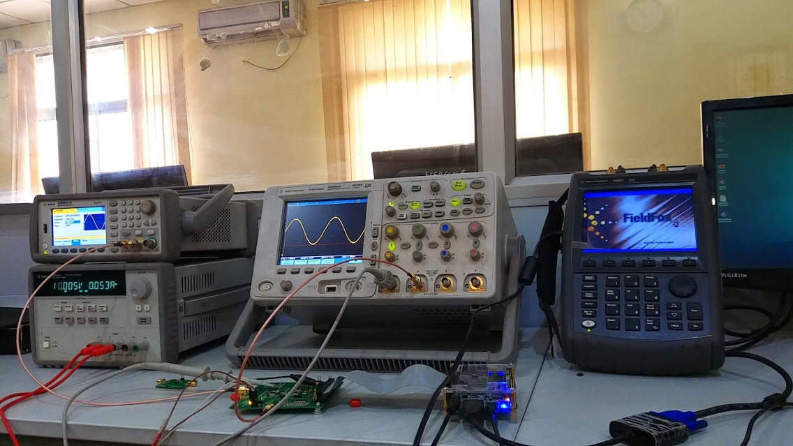
DAQ Testing
LNA and PA design
The working frequency of Power amplifier and Low noise amplifier is same. A bandpass filter precedes an LNA. LNA has internally terminated 50 Ohm impedance so external network of inductor and capacitor can be used as bandpass filter. We are using MGA-62563 from Broadcom technologies as LNA and PA both (Due to limit the complexity of design). The P1dB compression point of this amplifier is 18dBm which is sufficient for a peak transmit power of 15dBm (considering losses due to impedance mismatch at antenna & other).
RF Bias tee – In short, bias tees are diplexers which are used to provide clean voltage bias to the RF amplifiers. The high frequency part of the signals passes to ground using the capacitor while the DC component passes through the inductor into the device. \[\frac{1}{2\pi{f}C} << Z_0\]
\[2\pi{f}L >> Z_0\]
Here \(Z_0\) is the characteristic impedance of the device. LNA is simply a device most of the time composed of a single or double BJTs. The devices need biasing for proper operation. The low frequency port of the bias tee provide the required bias. We choose values of capacitors and inductors more than 10-15 times higher than the minimum required value from the aforementioned values.
More info coming soon ..

Mixer
A passive mixer is used to find the beat frequency. When a mixer is used for down-conversion, the input is the RF signal and the output is the IF; for up-conversion the opposite is true. Conversion loss is a measure of the efficiency of the mixer in providing frequency translation from the RF input signal to the IF output signal. For given RF and LO frequencies, two nominally equal amplitude output signals are produced at the sum and the difference of the RF and LO frequencies. These two outputs are called side-bands.
This application note (Source : Mini-Circuits) contains all important terms & their definitions related to mixers.
We have chosen HMC688/9 for making the mixer board. It is a passive mixer having good linearity than an active mixer. As per the datasheet it requires less power in the input of LO (as there is already a amplifier int the input of the LO).
Antennas
We have decided to use microstrip planar antennas for transimssion of electromagnetic waves. Our current requirement is high gain and low VSWR while maintaining a 300MHz bandwidth. The bandwidth requirement is important because the frequency sweep is required for the FMCW to work. We would evaluate following antennas for our project.
- Rectangular patch antenna
- Vivaldi UWB antenna
Microstrip patch antennas have advantage of portability, ease of manufacturing, low-cost, easy to simulate in simulation software for pre-fabrication tuning and analysis. Array of patch antenna can also be fabricated with ease using the same methods which can improve its gain & directivity.
The simulation software we are using is ANSYS Electromagnetic suite 19.0 (HFSS). Substrate Material we are using is FR4-Epoxy (\(\epsilon{}_r = 4.4\)). We have used following online calculators for patch antenna design (Source : Pasternak Enterprises Inc.) :
a. Microstrip patch antenna calculator
b. Microstrip impedance calculator
Of the various types of feeding a patch antenna we are using the microstrip line feed.
The following pre-requisite data have been compiled before & after the simulation for FR4-Epoxy substrate:
1. Width of the patch feed = 3.083mm
2. Gap between feed conductor and patch (microstrip line feed) = 0.4mm
3. Width of the patch = 36.34mm
4. Length of patch = 28.11mm
5. Feed length (from edge of the patch) = 11.0275mm
6. Copper thickness = 0.035mm
7. Substrate thickness = 1.6mm
8. Wavelength = 57.5mm
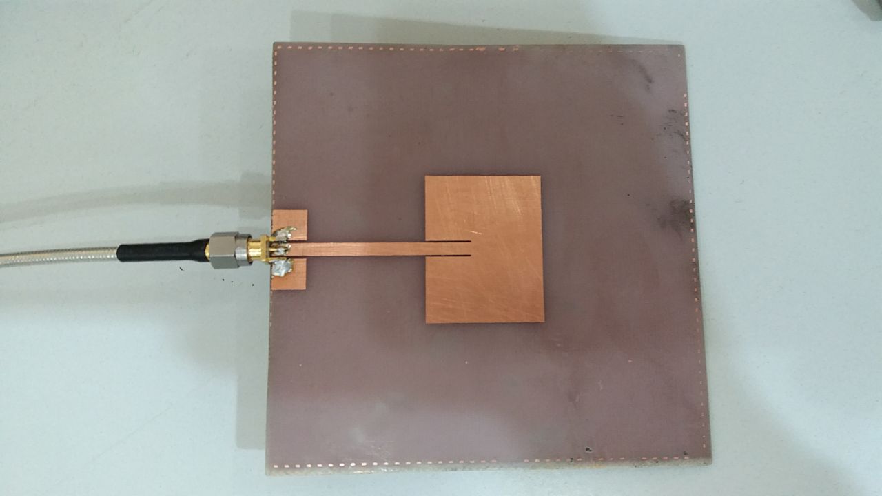

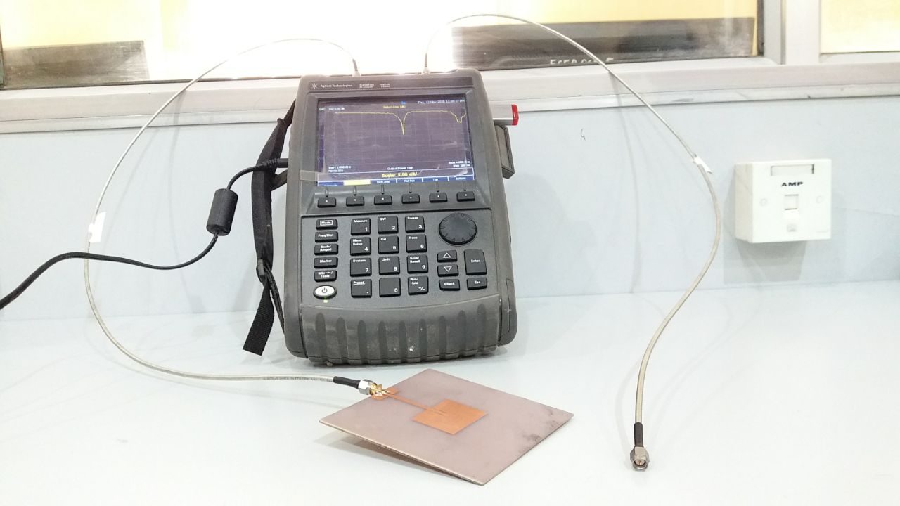

The result of the fabricated antenna match with the calculated value. However it slightly deviates from the simulated results. It may due to some inaccuracies in the parameters we put above. However the deviation is less than 66MHz which confirms the match of 50 impedance line and dielectric constant value of FR4 Epoxy substrate.
Planar Directional Coupler
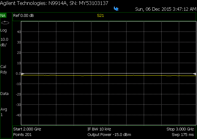

The isolation is not very good (almost equal to coupling, hence zero Directivity). However it is enough for our application where we need very little power to be drawn from the main line so that maximum power enters the antenna.
Basics of the directional coupler can be found here.